
The scale and urgency that continue to characterize TSMC’s trajectory reshape the semiconductor industry. US$38–42 billion was invested in capital expenditure in 2025, about 70% of which was channeled into advanced process development. Aggressive investments underpin its foray into 2-nm technology mass production in the second half of 2025, working toward up to 90,000 wafers per month by late 2026. For AI workloads, the projected 25-30% energy efficiency improvement over 3nm nodes is, again, not just incremental but crucial to sustaining performance gains without runaway power costs.
1. Engineering the 2nm Leap
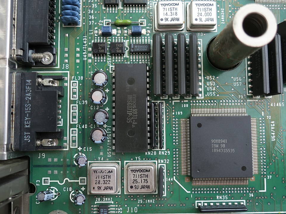
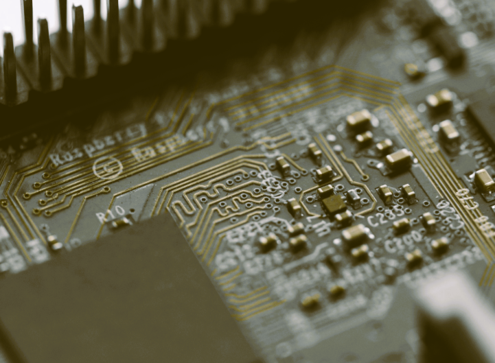
TSMC’s N2 node implements gate‑all‑around transistor architecture and, with future generations, backside power delivery. GAA uses nanosheet structures instead of FinFET designs to enhance electrostatic control and allow higher drive currents with less leakage. BSPD relocates power lines to the back side of the transistor layer, freeing up routing resources for signals and reducing voltage drop. Early N2 production will skip high‑NA EUV lithography to avoid supply constraints of the $370‑million scanners that ASML can manufacture in only single‑digit quantities each year. The move accelerates deployment but cuts the full performance potential of N2 until the A16 process (1.6nm) arrives in 2027.
2. Advanced Packaging: CoWoS and SoIC Expansion
TSMC’s packaging roadmaps are every bit as important as its process scaling roadmaps. CoWoS capacity will rise from 13,000 to 110,000 wafers per month by 2026, but demand-fueled by the NVIDIA H200 and B100 accelerators-continues to outstrip supply. CoWoS integrates high-bandwidth memory and logic dies using large silicon interposers for the bandwidth and thermal headroom that AI GPUs require.
SoIC is the 3D-IC stacking technology of TSMC, which reduces interconnect paths between dies and further improves latency and power efficiency. A modular design language called 3Dblox enables the heterogeneous integration of chiplets across process nodes, an increasingly important attribute for domain-specific AI accelerators.
3. Global Expansion and Supply Chain Resilience
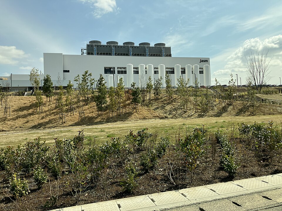
Unprecedented overseas build‑out for TSMC includes $165 billion in the U.S. for three fabs, two advanced packaging plants, and an R&D center in Phoenix, plus a deepening footprint in Japan through JASM with Sony and Denso. Arizona’s Fab 21 already produces 4nm wafers for NVIDIA’s Blackwell GPUs; future phases will bring 3nm and 2nm production stateside. Japan’s Kumamoto fabs focus on mature nodes for automotive and industrial markets, with potential expansion into advanced packaging. These moves help diversify geographic risks and align with “friendshoring” incentives under the U.S. CHIPS Act.
4. Geopolitical risk concentration
At the same time, over 90% of TSMC’s wafer capacity is still within Taiwan, including all current 3nm and planned early 2nm production. Putting such a huge amount of concentration risk on the AI hardware supply chain relative to Taiwan Strait tensions, which have worsened, with military exercises in 2025, would potentially bring 90% of leading-edge chip output to a halt and take out AI compute globally. None of the three competitors-Samsung, Intel, SMIC-are positioned to match N2-class yields at scale prior to 2027, leaving no viable backup for NVIDIA, AMD, and Apple’s flagship products.
5. Competitive Packaging Alternatives
Capacity constraints in CoWoS have opened a window for Intel’s EMIB and Foveros packaging. In comparison to full interposers, EMIB links chiplets using embedded silicon bridges at much lower cost and without the thermal complexity for inference-class ASICs. Foveros achieves high-density heterogeneous integration through vertical die stacking that is enabled by either through-silicon vias or hybrid bonds. Intel scales EMIB 30% and Foveros 150% in its Rio Rancho facility while MediaTek and Marvell show interest and, possibly, Apple and Qualcomm hedge their bets in case CoWoS bottlenecks persist.
6. AI Hardware Dependency:
Process leadership by TSMC sets the cadence for AI hardware innovation. NVIDIA’s H100, H200, and Blackwell GPUs; AMD’s MI300 accelerators; and Apple’s latest SoCs all tap into TSMC’s leading‑edge nodes and packaging. For large language models in autonomous systems and HPC workloads, energy efficiency gains at 2nm save data center cooling costs while pushing more throughput per rack. Without TSMC’s capacity, AI hardware roadmaps would be delayed several years.

7. Technology Roadmap into the Angstrom Era:
Beyond N2, TSMC’s A16 node in 2027 will introduce BSPD with high‑NA EUV, taking transistor scaling into the angstrom range. This roadmap aligns with Intel’s 18A and Samsung’s SF1.4 nodes, but TSMC’s ecosystem depth-process design kits for every packaging option, broad EDA integration, and the largest base of advanced‑node customers-remains unrivaled.
The foundry’s ability to deliver complete solutions, from logic to memory integration, makes it a default choice for bleeding‑edge AI silicon. TSMC’s scale, technology leadership, and geopolitical centrality make it both the backbone and the bottleneck of global AI compute. For investors and industry strategists, the next 24 months-covering N2 ramp‑up, CoWoS expansion, and overseas fab progress-will determine whether the company can sustain its dominance while mitigating the single‑point‑of‑failure risk embedded in Taiwan’s silicon crown jewels

